Conductors, Insulators, and Semiconductors:
All materials have electrical properties that allow them to be organized into three broad categories: conductors, insulators and semiconductors. Metals (pure elements and alloys) are typically conductors of electricity. Thousands of miles of aluminum and copper wires crisscross the country bringing electricity into our homes and places of work. A relatively small number of nonmetallic substances can also be classified as conductors. Also, a very few ceramic compounds have exhibited the unusual property of superconductivity at the frigid temperature of liquid nitrogen or below. The nonmetallic elements and their compounds fall into the class of electrical insulators. Most ceramics and plastics do not conduct electricity under ordinary circumstances. Plastic coatings are frequently found covering copper wires to protect the user from shock and keep devices from short circuiting. Ceramic knobs are used where electrical wires are attached to utility poles or to the back of a house. The third group of materials, the semiconductors, can be understood from their name, to fall somewhere midway between conductors and insulators.
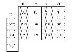
Although pure elements such as silicon play an important role in many semiconductor devices, it is most often utilized by adding very small but controlled amounts of impurities in order to alter its properties. Silicon-based materials dominate in the semiconductor industry and in electronic devices like computers and calculators, but a number of other compounds are also used extensively--including GaAs (or gallium arsenide) which is the material used in the laser of a CD player. Some other combinations of elements that exhibit semiconductor properties are indicated on the periodic table below (See Figure 1). In the readings and lab activities that follow, the emphasis is on what semiconductor materials are, how they are used, what properties they possess, and why they behave as they do.
Figure 1: Elements found in elemental and compound semiconductors. Group IV are elemental semiconductors. Compound semiconductors can be formed by combining Groups III and V or II and VI.
Electrical Conductivity:
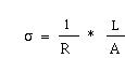
Electrical Conductivity is a function of a material's ability
to carry an
electrical current. The conductivity (![]() ) of a material is
determined
by taking the reciprocal of the measured electrical
resistance (R) to
the flow of electricity in a length (L) of material divided by the
cross-sectional area (A).
) of a material is
determined
by taking the reciprocal of the measured electrical
resistance (R) to
the flow of electricity in a length (L) of material divided by the
cross-sectional area (A).
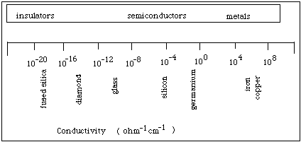
See Figure 2 for comparisons of conductivities in materials. Conductivity is temperature dependent. As the temperature increases, the conductivity of a metal decreases. In contrast, the conductivity of pure semiconductors and insulators increases as the temperature increases. Controlling and changing the conductivity of materials is one of the challenges facing electronic material scientists.
When an electric field is applied, electrons may flow through a material if there are empty states in the outer (valence) shells of the atoms that make up the material. An electron will not easily transfer between atoms if there is not a vacant state of similar energy in the receiving atom for it to occupy. We model the empty and filled states (electron energy levels) using quantum theory. A single atom has electrons localized about itself. An atomic orbital of one atom may overlap with an atomic orbital of another atom forming two molecular orbitals. One, called the bonding molecular orbital, is of low energy and the other with higher energy is called the anti-bonding molecular orbital. As more and more atoms assemble to form a solid, the number of bonding and anti-bonding orbitals of about the same energy increases, and they begin to take on the characteristics of an energy band. (See Figure 3). The energy differences between orbitals within a band is slight. Electrons can move freely among these orbitals within an energy band as long as the orbitals are not completely occupied. The highest occupied energy band is called the valence band. But, there is a region that separates the valence band from the conduction band where there are no orbitals. Electrons are not allowed to have these energies. In insulators, this energy gap is relatively large and in semiconductors, the energy gap is intermediate.
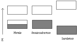
Figure 3: The energy bands of metals, semiconductors and insulators. For the insulators and semiconductors, the lower band is called the valence band and the higher band is called the conduction band. The lower energy band in metals is partially filled with electrons.
Atoms that form metallic conductors have many partially and fully unoccupied levels with similar energies: a large number of mobile charge carriers are able to move across the material when an electrical potential (voltage) is applied. In a semiconductor or an insulator, the valence band is completely filled with electrons in bonding states so that conduction cannot occur. There are no vacant levels of similar energy on neighboring atoms. At absolute zero, its anti-bonding states (the conduction band) are completely empty. There are no electrons there to conduct electricity. This is why insulators cannot conduct. In the case of semiconductors, as temperature increases, electrons in the valence band acquire sufficient energy to be promoted across the "energy gap" into the conduction band. When this occurs, these promoted electrons can move and conduct electricity. The smaller the band gap, the easier it is for electrons to move to the conduction band.
An Analogy:
An analogy to explain this conduction process might help. Imagine a superhighway in Los Angeles with four local traffic lanes and four express lanes going north (the direction opposite the electric field). Now imagine that construction has stopped traffic in all the express lanes (valence band). Meanwhile the local traffic lanes (the conduction band) are totally empty because everyone decided to take the express lanes to go faster. No one can move on the express lanes, and there are no cars on the local lanes so no one gets anywhere. Suddenly, the LA Raiders football team (heat energy) gets out of another bus stuck in the traffic and decides to lift cars over the barrier (the energy gap) into the local lanes. The higher the barrier is, the slower the team will lift cars over the barrier, and the fewer cars get to move. Every time a car is lifted over the barrier, it gets to move so "current flow" begins. Every time a car is removed from the express lane, other cars can move into the hole it leaves, so some current also gets carried there (in the valence band). Notice that the car in the local lanes moves in the opposite direction from the hole left behind! Unfortunately, the cars in the local lanes get off at exits from time to time and more cars come into the express lanes to fill the holes so only a limited amount of current can flow.
This analogy works well to explain conduction in pure (intrinsic) semiconductors in which the charge carriers come from the chemical bonds in the substance itself. Heat energy in a semiconductor increases the number of electrons promoted into the otherwise empty conduction band; the vacancies (or holes) created in this process allow mobility of electrons in the valence band through the material. At high temperatures these semiconductors are relatively good conductors because there are a larger number of electrons in the conduction band and holes in the valence band available for electron movement. But at low temperatures, intrinsic semiconductors are insulators since the number of electrons and holes is diminished. At absolute zero, an intrinsic semiconductor would have no electrons in the conduction band. However, the most important semiconductors are of the extrinsic type, where some impurity (another element) has been intentionally added in the solid to increase the conductivity. The properties of an extrinsic semiconductor are governed by the presence of these impurities.
Doping:
Doping can produce two types of semiconductors depending upon the element added. If the element used for doping has at least one more valence electron than the host semiconductor, then an n-type (negative type) semiconductor is created. For example, if arsenic is added to a silicon crystal, the arsenic has one more valence electron (5) than silicon (4). That extra electron is available to carry a current. So an As atom in Si is like a car that decides to get onto the local lanes of the LA freeway since the express lanes are clogged. With silicon or other Group IV semiconductors, any member of Group V (nitrogen is not used) could form an n-type semiconductor. If the semiconductor is doped with an element having at least one less electron than the host material, then a p-type (positive type) semiconductor is formed. As an example, if silicon is doped with aluminum (three valence electrons), a hole will be formed in the valence band. Again any member of Group III could dope a host semiconductor from Group IV and show the same effect. The solid would have a "positive" hole in its electronic structure that would move in the opposite direction of the electron flow . Thus a p-type semiconductor would be formed. This would be as if the football team picked up a car and placed it on the median between the express lanes and the local lanes. Doping cannot be done to the point where it disturbs the crystalline structure of the host semiconductor. Doping is done in the range of parts per million concentrations, but may be up to a few parts per thousand. A semiconductor doped to several parts per thousand level has a conductivity close to that of a poor metal. Thought question about Figure 4: Why are the levels of the n-type and p-type dopants slightly different from the levels in the intrinsic semiconductor?
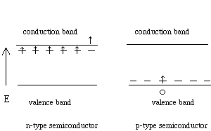
Figure 4: A p-type and n-type semiconductor. The fifth valence electron of the n-type dopant can easily jump to the conduction band and carry current. In the p-type semiconductor, electrons are easily promoted to the vacant level in the dopant. This creates a hole in the valence band which can carry current by traveling in the opposite direction of electron flow.
Hole Concept:
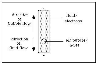
A couple of additional analogies might help to explain the hole concept. For the first one, you will need six chairs and five students. Line up the six chairs and have the five students sit in a row leaving the chair on the right vacant. Assume that the outside current terminals are positive to the right and negative to the left. As the flow of excited electrons moves through the crystal toward the positive terminal, so electrons from a bonded site move toward the positive terminal into an adjacent hole causing the hole to migrate toward the negative terminal. Have the students (electrons) move one chair toward the right; notice that the empty chair (positive hole) has moved, effectively to the left.
The second demonstration requires a glass test tube filled with glycerin and stoppered. Be sure to leave an air bubble inside the stoppered tube. The glycerin represents the electrons and the air bubble represents the positive holes. As the tube is inverted and the electrons move in their direction (down - due to gravity in this case but due to the positive terminal in an electronic scenario), the air bubble moves in the opposite direction ( up - due to density differences in this case but due to attraction toward the negative terminal in the electrical case.) After these two demonstrations, it should be clear that the semiconductor holes and electrons move in opposite directions.
Application and Research:
The building block of most semiconductor devices involves combining p-type and n-type regions into p-n junctions. Imagine bringing together two crystals where one is n-type and the other is p-type. A few of the electrons from the n-type flow toward the p-type material. At the point where the p-type and n-type meet (the interface) electrons from the n-side fill the holes on the p-side and a build-up of oppositely charged ions is generated, and thus a potential across the barrier forms. This build-up of charge is called the junction potential. The barrier prevents further migration of electrons and the net current is zero.
If a voltage is applied to the p-n junction with the negative terminal connected to the n-region and the p-region is connected to the positive terminal, the electrons will flow toward the positive terminal, while the holes will flow toward the negative terminal. This is called forward bias and current flows. However, if the positive terminal is connected to the n-type and the negative connected to the p-type, a reverse bias forms and no current flows due to the build up of the potential barrier. In other words, these devices must be placed in an electrical circuit with the correct polarity, or they will not function. This application of the p-n junction is used in many electronic devices. Figure 6 shows the formation of a potential at a p-n junction. Figure 7 shows the effect of forward and negative bias on the p-n junction.
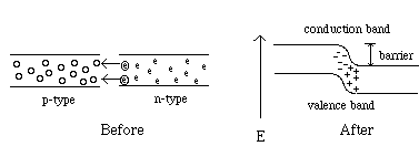
Figure 6: A p-n junction before and after the two materials are brought in contact. When the two materials are placed together, electrons from the n-side combine with the holes on the p-side. This results in a positive charge on the n-side of the junction and a negative charge accumulation on the p-side. This separation of charge creates a junction potential. Note: There are no electrons or holes at the junction, they have combined with each other.
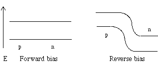
Figure 7: A p-n junction under forward and reverse bias. Notice that in forward bias, the barrier is lowered, while in reverse bias, the barrier is raised.
Thought question: In each case in Figure 7, which side is connected to the positive terminal of the outside voltage source? Will electrons or holes carry current when the junction has this arrangement ?
Electronic Devices:
There are many electronic devices that function using combinations of p-n junctions such as diodes, solar cells and transistors. In this section a brief explanation of each of these basic devices will be given.
The diode is a p-n junction application that acts as a rectifier for converting alternating current to direct current. This is due to the ability of a diode to allow current flow in one direction but not in the other.
Solar cells are p-n junction devices which use sunlight to create electrical energy. It is the energy of the sun`s photons that causes the electrons to be promoted into the conduction bands and carry the current. However, the current derived from the solar cell is small. It takes many solar cells to produce enough current to do a large scale job. If the energy output from solar cells could be increased, solar energy could be used for more than individual, isolated applications.
Transistors are another application of the p-n junction. Transistors, unlike diodes, contain more than one p-n junction. Because of this, a transistor can be used in a circuit to amplify a small voltage or current into a larger one or function as an on-off switch. Transistors are of two main types: bipolar junction transistors (BJT's) and field effect transistors (FET's). Roughly 95% of all electronic systems utilize one or both of these types of devices.
BJTs are composed of three layers of doped materials, either n-p-n or p-n-p in configuration. The BJT acts like a bump or dam in an open stream to control the amount of current let by; thus as the bump is lowered, more current can flow. In the BJT, the height of the bump is controlled by the base current in the semiconductor. The BJT was invented in 1948 by John Bardeen, Walter Brittain and William Shockley using germanium. BJT's remained the only important three terminal semiconductor devices for about a dozen years after their invention, and helped to launch the modern electronics era.
Since the early 1960's the FET has been considered one of the most important devices in solid state technology. At present, many of the applications of BJTs have been taken over by metal-oxide semiconductor FET's (MOSFETs). MOSFETs were theorized for many years before they were able to be manufactured. The reason MOSFETs could not be made was that scientists had not yet developed techniques for growing high quality silicon dioxide (SiO2) on silicon. The FET functions more as a gate for controlling the flow of current (like a valve on a faucet). FET's are relatively simple to fabricate compared to BJT's, and they have proven to be extremely fast, reliable switches in miniaturized circuit components with much less power usage than BJT's. Most modern microprocessors are based on FET devices--from pentium chips in PC's to the CPU's of super computers. Transistors, diodes, and other electronic devices are combined in many different patterns to form today's integrated circuits.
The integrated circuit (IC) has been the workhorse of the "microelectronics era" which began in the late 1950's. These chips, usually made of silicon, consist of combinations of four fundamental electrical regions. These regions contain resistors, capacitors, diodes and transistors. Since 1971, Very Large Scale Integration (VLSI) has allowed millions of such regions to be fabricated on a chip that is only one square centimeter. Not only are these circuit elements getting smaller, they are getting faster as well. For example today's typical desktop pentium-based computer can perform tens of millions of operations per second, whereas contemporary super computers are rated in gigaflops (billions of operations per second). Teraflop (trillions of operations per second) machines will be ready for production by the year 2000.
Properties and Processing of Electronic Materials:
The dominance of electronic materials in this present information age is due in part to several fundamental scientific discoveries in the nineteenth century. Most modern semiconductor-based devices require the chemical elements silicon, germanium or gallium (combined with arsenic), but none of these had been isolated or identified prior to 1824. Though silicon is the second most abundant element in the earth's crust, it proved very difficult to separate from its natural compounds such as silicon dioxide in ordinary sand and other silicate minerals. Through persistence and ingenuity, a Swedish chemist named Berzelius finally obtained the elusive silicon. He reacted silicon tetrafluoride with potassium metal and chemically reduced it from its compound in order to obtain the element silicon for the first time.
Over ten thousand times more rare than silicon, the existence of gallium and germanium had not even been suspected until the table of elements was proposed by Mendeleev in 1868. Within two decades, the discovery and characterization of these elements clearly showed the periodic table to be a tool, not only for recording chemical information but also for predicting the results of chemical research. Finally, it was these same two elements along with silicon that provided the testing ground for the investigation of semiconductors several decades later.
According to very general trends of properties on the periodic table, it can be demonstrated that elements increase in metallic character when going to the left of a period (row) or down a family (column). Thus it would be expected that the most metallic of elements would be found at the lower left corner of the table and the least metallic at the upper right. This is made quite obvious by displaying an illustrated periodic table. There is a gradual transition of properties from metallic to nonmetallic in going to the right across a period and up a family. A line of division is commonly placed on the table which looks like a stairstep pattern with the elements falling on either side of this line being loosely classified as semiconductors. See Figure 8.
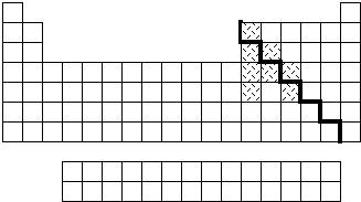
Figure 8: Periodic Table of the elements. The elements to the left of the bold line are metals and those to the right are nonmetals. The highlighted elements are elemental semiconductors or used in compound semiconductors.
At the center of the representative elements, Group IV (carbon family) elements have been found to have some very important properties that are intermediate between metallic and nonmetallic. Perhaps of greatest significance is the characteristic of being a semiconductor. Excluding lead (and tin below its transition temperature), all the other elements in the family can have their atoms arranged in the same way as those in a diamond (pure carbon). In this form, carbon has a very high resistance to the flow of electricity; thus it can be said to be a poor conductor and is classified as an electrical insulator. At the other extreme, tin, in its common crystal arrangement at room temperature, has a relatively low resistance to the flow of electricity; thus it is a reasonably good electrical conductor when it is in its metal form. However, tin has a transition temperature above which it has a diamond crystal structure and is a much poorer conductor. Both pure silicon and pure germanium behave as perfect insulators at absolute zero (-273 � C), but at moderate temperatures their resistance to the flow of electricity decreases measurably. Since they never become good conductors, they are classified as electrical semiconductors.
When selecting a semiconductor material for electronic applications, a number of factors must be considered. Of primary importance is the inherent band gap size (the energy difference between the valence and conduction bands). Furthermore, the ordinary chemical and physical properties of the host material and its compounds play important roles as well. Silicon has the advantage of forming a protective surface oxide when heated in oxygen. Silicon also forms stable conducting compounds with many other elements, including metals, that help produce stable electical contacts to it.
Like carbon, silicon has four electrons that can be used for bonding, and it is referred to as tetravalent. Silicon forms several compounds that are analogous to those of carbon, for example, silane (SiH4) corresponds with methane (CH4), and silicon tetrachloride with carbon tetrachloride. In these compounds, both the carbon and the silicon are centered between the four other evenly spaced elements making the molecular geometry tetrahedral. In its extended compounds like the silicates in quartz, each silicon atom is surrounded by four oxygen atoms in an open tetrahedral network. When silicon is purified in its elemental form, it has a molecular geometry similar to diamond where each silicon atom is surrounded by four others which are surrounded by four and so on in an extended network.
Gallium arsenide materials are very useful in opto-electronics because they allow highly efficient absorption and emission of light. Future research will focus on maximizing the beneficial properties of each of these materials by mixing and layering them to improve opto-electronic sensitivity, power consumed and signal transfer rate.
There are two main steps in the manufacturing of semiconductor circuits for computers and other electronic devices, growth and fabrication. First it is necessary to grow near perfect crystals of the semiconductor material, which are cut into thin, flat disks called wafers. The second step, device fabrication, involves patterning the circuits, etching or depositing the circuit components on the wafer, and then sectioning the larger wafer into smaller chip size pieces called dies. Fabrication of devices can sometimes involve more than a hundred steps.
Crystal Growth:
Large, single crystals of semiconductors (Si and GaAs) are grown from the melt using the Czochralski technique. The raw material (as pure as possible) is placed in a crucible and heated to a temperature above its melting point. A seed crystal is placed in the molten semiconductor and withdrawn slowly in a rotating fashion. This method can be used to grow crystals as large as twelve inches in diameter. The final crystal is cylindrically shaped and must be cut into thin disks using a diamond-tipped saw. These wafers are then polished using a grit of very hard, small particles, such as silica (SiO2). Due to the nature of the solidification process, the final solid semiconductor is purer than the raw material that was used to produce it. See Figure 9.
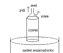
Figure 9: The Czochralski technique for growing single crystal semiconductors.
Circuit Fabrication:
After semiconductor wafers of sufficient purity have been manufactured, circuit elements must be placed at the surface. Circuit elements are added to the wafer using either etching or deposition. An example of the use of etching in circuit fabrication would be the etching away of a few thousand Angstroms (10 -8 cm) of the semiconductor between each device, effectively isolating the devices from each other. Because small mesas are formed as a result of this process, it is called mesa isolation. Most circuit elements, however, are deposited, implanted, or grown at the surface. These can include insulators (e.g.. SiO2 is grown in the fabrication of MOSFETS) or metals (e.g.. Aluminum is deposited in order to connect devices on a chip.) Dopants can be implanted at the surface of a wafer and allowed to diffuse into the material by heating it. Both etching and deposition require a process called photolithography. Figure 9 shows a typical photolithograpy process used for mesa isolation, and Figure 10 shows the depositing of a metal. After many devices have been formed on the wafer, they are separated into individual chips by a sectioning process.
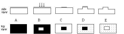
Figure 10: A typical photolithography process for the isolation of a device on a chip. In step A, a thin layer of a photosensitive polymer is placed on the chip. In step B, light selectively exposes a portion of the polymer. The unexposed portion is stripped off in a developing process in step C. The unprotected surface of the chip is etched away in a chemical process in step D. Finally, in step E, the remaining polymer is removed, leaving a mesa of unetched semiconductor, surrounded by an etched region.
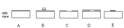
Figure 11: Depositing a metal on a semiconductor. In steps A and B, the chip is coated with a photosensitive polymer and light exposes the polymer in the region where the metal is to be placed on the chip. In step C, the exposed area is stripped off in a process called developing. Metal coats the surface in step D. This is done by vaporizing a metal and allowing the vapor to condense on the surface of the semiconductor. When the remaining polymer is removed in step E, metal remains only in the region unprotected by the polymer.
Semiconductor Summary:
Semiconductor devices now influence our lives on a daily basis. Although insulators and conductors are useful in their own right, semiconductors such as silicon and gallium arsenide have dramatically changed the way in which billions of people live. Their intermediate ability to conduct electricity at room temperature makes them very useful for electronic applications. For example, the modern computing industry was made possible by the ability of silicon transistors to act as fast on/off switches.
All materials have energy bands in which their electrons can exist. In metals, the valence band is partially-filled and the electrons can move through the material. In semiconductors, however, there is a band gap that exists, and electrons cannot jump the gap easily at low temperatures. At higher temperatures, more of the semiconductor`s electrons can jump the gap; and its conductivity goes up accordingly. Electrical properties can also be changed by doping (adding impurities to the semiconductor material). This too, is one of their great assets.
Putting impurities in a semiconductor material can result in two different types of electrical behavior. These are the so called n (negative) and p (positive) type materials. Group V elements like arsenic added to silicon or germanium produce n-type by virtue of their extra valence electron. Group III materials like boron produce the p-type since they have only three valence electrons. When n-type material is connected to a p-type material, the device exhibits diode behavior. That is, current can flow in one direction across the interface but not in the other.
Diodes not only act as rectifiers, they have also led to the development of the transistor. A bipolar junction transistor (BJT) is a diode with a third material added to create a second interface. Either npn or pnp types exist, but their basic operation is essentially the same as two diodes connected to each other. Proper biasing of the voltages across each diode of the device can allow for large current amplification. Today, metal oxide semiconductor field effect transistors (MOSFETS) have replaced the BJT in many applications. Now, millions of transistors can be placed on a single silicon chip or integrated circuit. These IC chips are more reliable and consume less power than the large vacuum tube circuits of the past.
There are two main steps to the fabrication of electronic devices from the raw materials. First, the semiconductor is melted and a seed crystal is used to draw a large crystal of pure, solid semiconductor from the liquid. Wafers of the semiconductor are sliced and polished. Next, the circuit pattern is etched or deposited using a photolithographic process. Finally, the individual chips are sectioned from the original wafer.
Electronic computing speed has also increased greatly with the integrated circuit. Cycle times of today's computers are now measured in nanoseconds. Opto-electronic (laser diode) research is extending the already huge rate at which information can be transmitted. All in all, semiconductors continue to drive technological progress into the 21st Century.